AMD manufactures its Ryzen chips at 7 nm, while Intel’s tenth-generation chips are built at 10 nm and 14 nm depending on the model. What do these nanometers actually mean, and what do they really say about a chip’s performance?
Intel’s tenth-generation processors include two very different chip families: there’s Ice Lake, manufactured at 10 nm, and Comet Lake, manufactured at 14 nm. AMD has its Ryzen CPUs built in TSMC’s factories at 7 nm.
There’s a lot of back-and-forth between Intel and TSMC regarding these nanometer designations. For example, what Intel calls 10 nm would be identical to what TSMC describes as 7 nm. The distinction is important: the size of a production node has a direct impact on chip performance. Now that Intel has muddied the waters with its tenth generation and AMD is once again a relevant competitor, we’re examining what these nanometers actually mean.
About Nodes
The collective term for the technology used to make a chip is a ‘node’. Nodes are distinguished from each other by a naming convention in nanometers. 14 nm, 10 nm, 7 nm… are production nodes. They give an indication of the precision of the production process in a factory. For example, Intel has chip factories that produce chips on a 10 nm node, which means that these chips are manufactured using a collection of modern technology that falls under the ’10 nm’ umbrella.

A common misconception is that the nanometers refer to the size of the transistors on a chip. Today, this is not the case. Until 1997, there was a direct relationship between the size of a transistor and the naming of a node. Specifically, a node corresponded to the length of the transistor gate produced with the technology.
The 350 nm node in 1995 got its name because of chips with transistors with a gate length of 350 nm that rolled off the 350 nm node production line. Around the turn of the century, this relationship was lost. New technologies for building microtransistors led to higher transistor density on microchips, making gate length no longer the relevant factor.
Fewer Players, more Differences
Until about 2013, there was consensus in the processor world about what a specific node should entail. Because it takes an average of almost 15 years to get technology from a scientific paper into an operational chip factory, until then there was an overarching industry body that developed long-term roadmaps for processor nodes. The ‘International Technology Roadmap for Semiconductors’, ITRS for short, set goals for each node regarding the number of transistors per chip and the average size of components on such a chip.
In recent years, the ITRS has been reformed and the roadmap has become much less relevant. Logical: where chips were previously built in factories of about a dozen manufacturers, today there are only three companies that can set up production lines with the most modern technology: Intel, Samsung and TSMC.
GlobalFoundries stalled at the 14/16 nm node and failed to successfully scale its factories to 10/7 nm. Changing nodes is indeed a costly affair, both in terms of research and materials. Billions of euros are involved in shrinking a node.
Hijacked by Marketing
If the nanometer designation no longer corresponds to a specific component on a chip, and it’s also not an umbrella term under which conventions in terms of size and technology hide, what are terms like 14 nm and 10 nm still worth?
The nanometer designation for nodes has now been taken over by the marketing department.
On a technical level, very little. The nanometer designation for nodes has now been taken over by the marketing department and no longer has any direct relation to components of a microchip. If Intel goes from 14 nm to 10 nm, you can’t deduce from that what exactly happens in the production process.
Indicative Term
Today, the node size is more of an indication that a chip maker has equipped its factories with new technology, which is more precise at various levels and allows for higher transistor density. How much more precise is not entirely clear.
Historically, a new node should be accompanied by a doubling of the number of transistors on a given area, but even this rule of thumb is little more than a rough indication today. When a node shrinks from size X to size Y, the manufacturer mainly indicates that a big leap forward has been made in its own production process.

What that production process exactly is differs more than ever between different factories. Intel builds its chips differently than TSMC and Samsung. Various technologies related to a scale change are introduced at different times (FinFET, Gate-last..). This means that a chip designer today must work closely with their manufacturer of choice.
Chip designs must be optimized more than ever not only for the node used, but for the implementation of that node by TSMC, Intel or Samsung. Anyone wanting to have a design created for Samsung, for example, made in a TSMC factory on a similar node, can expect a small year of redesigns.
Comparing
Looking at one manufacturer, the naming of a node is still valuable. 10 nm is better than 14 nm, and the improvements are big enough for the chip maker to speak of a new node. This typically means more compact components on the chip, which leads to better performance. We’ll explain exactly why later in the article. In any case, you can say without doubt that Intel’s 10 nm Ice Lake chips are structurally superior to the 14 nm Comet Lake processors.
10 nm is better than 14 nm. Surprise?
Making a comparison between manufacturers has become more difficult. AMD’s 7 nm Ryzen chips are baked by TSMC. A smaller node leads to better chips, but node names are the property of the marketing department. Is 7 nm at TSMC therefore really smaller than, for example, 10 nm at Intel? The latter claims vehemently that what TSMC calls 7 nm is actually just 10 nm by Intel convention. The Ryzen chips should be equivalent to Ice Lake processors in terms of production process.
The Numbers behind the Node
To investigate the claim, we opened Pandora’s box. 10 nm, 14 nm and 7 nm may be marketing terms, but they nonetheless correspond to certain specifications that are technically relevant. Specifically, it’s about the Contacted Gate Pitch and the Minimum Metal Pitch. The Contacted Gate Pitch is roughly the minimum distance between transistors on a chip, while the Minimum Metal Pitch is the minimum distance between the interconnects that connect transistors into logical circuits.
A smaller distance between transistors means a higher transistor density, a smaller distance between the interconnects means that you can also connect the extra transistors into more complex circuits. Under the node marketing flag, TSMC, Intel and Samsung neatly document their Contacted Gate Pitch and their Minimum Metal Pitch.
Looking first at 10 nm, we see that these distances for Intel are 54 nm and 36 nm respectively. TSMC’s 10 nm chips have a lower density: Contacted Gate Pitch and Minimum Metal Pitch are 66 nm and 44 nm. The same goes for Samsung, where the values are 68 nm and 48 nm.

If we now look at the 7 nm specifications, we see that TSMC and Samsung have reduced the two parameters. TSMC boasts 55 nm and 40 nm, Samsung 54 nm and 36 nm. Now compare with Intel’s 10 nm specifications, and you’ll see that the most important parameters for density at 7 nm at TSMC and Samsung indeed correspond to the specifications of 10 nm at Intel.
In other words: 10 nm Intel is comparable to 7 nm TSMC and Samsung. Put differently: Intel’s marketing department has missed the mark. There are other parameters that are relevant to assess the quality of a node, but they follow the same line.
Smaller, but why Better?
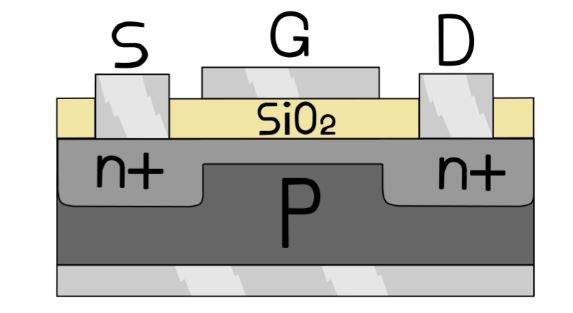
This brings us finally to the heart of the matter: why is smaller better? Higher density (of which Contacted Gate Pitch and Minimum Metal Pitch are thus good objective parameters) is generally associated with smaller transistors. A smaller transistor has a smaller distance between source and drain. This means that a lower voltage is needed to switch the transistor from 0 to 1 and vice versa.

A chip with an identical design, baked on a smaller node, will thus draw less power than its predecessor. This has a direct impact on battery life in laptops on the one hand, but also enables better performance on the other. With lower consumption, the generated heat also decreases. Because chips on a smaller node inherently run cooler than identical chips built on a larger node, they can handle slightly higher frequencies at the same TDP (thermal design point = maximum power consumption). The architecture (changes to chip design that are not related to the node) also has an impact, but research recently showed that it’s quite small.
Drawing Conclusions
That’s why you can say that Intel’s Ice Lake is inherently better than Comet Lake, without knowing the details of the node: smaller is always physically better. The chips are both baked in Intel factories and are thus comparable to each other.
For the same reason, you can’t say anything about Ice Lake versus AMD’s Zen 2 Ryzen chips based solely on the node. 7 nm seems smaller than 10 nm, but as we detailed above, that’s not always true in processor land.
Finally, EUV deserves a mention. Extreme UV refers to the wavelength used in the lithography process by which processors are made. You can compare this wavelength to the brush thickness in painting: the finer, the more precise the production process can be. Current nodes are already so precise that it’s difficult to build brushes that are fine enough. EUV technology promises to be a leap forward in this respect that will once again accelerate node shrinkage.
